


1. INTRODUCTION
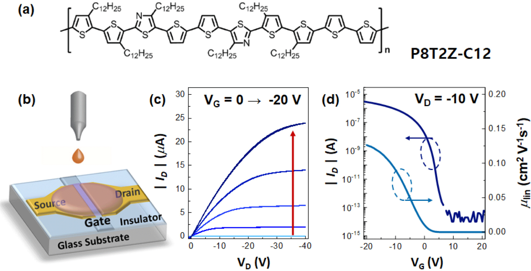
Organic printed electronic devices, which are made by directly printing functional organic semiconductor inks onto flexible substrates, have been investigated extensively for next-generation flexible electronics because of their mechanical flexibility and the potentially low cost of manufacturing them using graphic-art printing techniques [1-6]. Among the various printed electronic devices based on π-conjugated polymer semiconducting materials, polymer thin-film transistors (PTFTs) have shown considerable potential for widespread use as crucial building blocks for logic, arithmetic, and memory circuits for future electronic systems [2-4]. However, despite their considerable potential, the electrical instability of PTFTs caused by bias stress remains a major problem that needs to be addressed and solved to enable further developments of PTFT technology [3,7–9]. Here, we report an investigation of the effects of bias stress on the density of states (DOS) in PTFTs with electron donor–acceptor type conjugated copolymers of poly(tetryldodecyloctathiophene-alt-didodecylbithiazole)−P8T2Z−C12[the chemical structure is shown in Fig. 1(a)]−which were inkjet-printed to form an active channel layer [10]. The threshold voltage (VT) of the inkjet-printed PTFT shifted in the positive direction when the gate of the PTFT was subjected to positive bias stress (PBS), whereas it shifted in the opposite (negative) direction when the gate bias (VG) was removed. We analyzed the effect of the bias stress manifested by the VT shift by monitoring the device parameters and the DOS extracted from a combination of generation–recombination current spectroscopy, multi-frequency capacitance–voltage spectroscopy [11,12], and current–voltage (I–V) modeling [13–15]. The extracted subgap DOS revealed that the subgap states of the acceptors in the active channel strongly affect the VT shift of the inkjet-printed PTFTs during operation. We also dis cuss the physical mechanism of the electrical instability induced by bias stress in terms of the subgap DOS.
2. METHODS
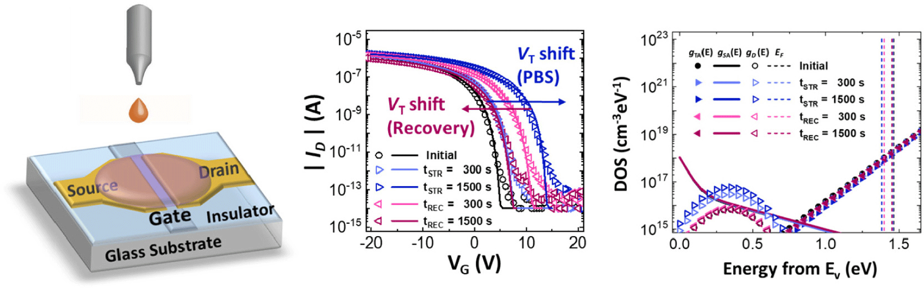
We measured the electrical properties of P8T2Z-C12-based inkjet-printed PTFTs using a bottom-gate, coplanar, structured device without any passivation to accelerate the electrical degradation, as shown in Fig. 1(b). Except for the passivation process, we fabricated the inkjet-printed PTFT as described previously [3]. We performed the electrical measurements under ambient conditions (relative humidity 30%) using an Agilent 4284A LCR meter and a 4156C semiconductor analyzer.
3. RESULTS AND DISCUSSION
Fig. 1(c) and Fig. 1(d) show representative output and transfer curves, respectively, of the inkjet-printed P8T2Z-C12 PTFT. The output characteristics show reasonable saturation with low hysteresis. As the drain bias (VD) increases, the output current, ID, becomes larger than ~25 μA at VD=−40 V and VG=−20 V. The transfer characteristics exhibit p-type behavior, with on/off ratios exceeding ~107. The curves of the mobilities with respect to VG show that the mobilities in the linear region (VD ≤ −10 V) increase gradually with VG and reach 0.13 cm2V−1s−1 at VG=−20 V.
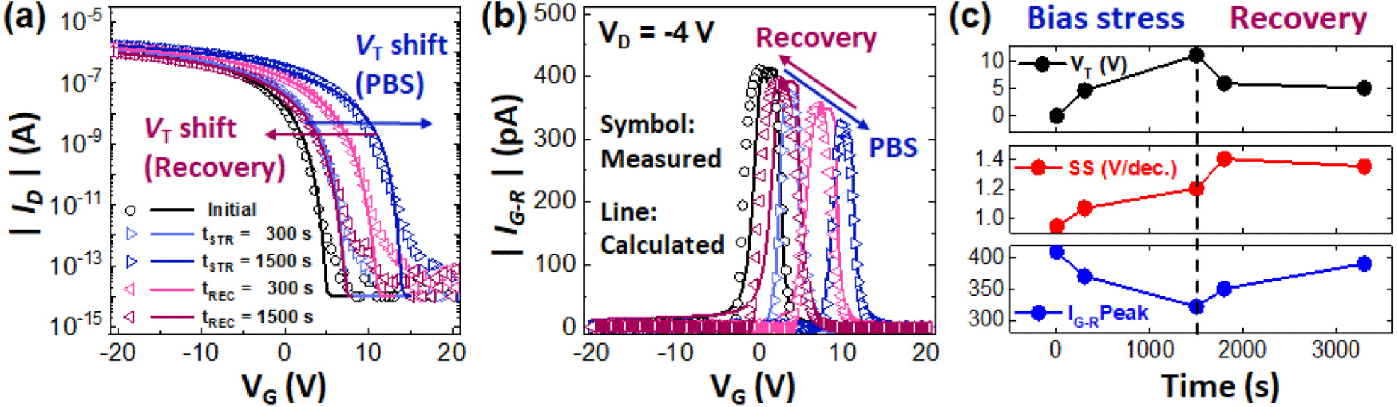
Fig. 2(a) and Fig. 2(b) show semilogarithmic-scale transfer curves at VD=−4 V and the corresponding generation–recombination (IG–R) currents as a function of VG for the inkjet-printed PTFT during PBS at VG=20 V and VD=−10 V together with the recovery obtained by releasing the VG from the PTFT. The symbols in the graph are from the electrical measurements, and the lines are from calculations based on an I–V model [13-15]. As shown in Fig. 2(c), when the PTFT is subject to PBS at VG=20 V and VD=−10 V, VT moves toward more positive values. This means that charge carriers are trapped either in the P8T2Z-C12 polymer layer or at the interface during operation, which consequently shields the gate potential, thereby inducing the VT shift. The trapping of negative electrons results in the positive shift of VT. However, VT recovered (i.e., moved in the negative direction) as the recovery time increased. In addition, the subthreshold swing (S.S.) increased as the duration of the bias stress increased, and it then decreased slightly with increasing recovery time.
The dependence of the changes in these characteristics of the inkjet-printed PTFT upon the duration of the PBS and of the recovery process can be analyzed quantitatively through a physical model based on the full-range DOS. To investigate the effects of bias stress in the PTFTs, we therefore obtained the profiles of the full-range DOS by applying various extraction techniques.
We modeled the DOS function [g(E)] in the bandgap of the P8T2Z-C12 polymer channel as a combination of a donor-like DOS [gD(E)], which includes donor-like tail states [gTD(E)] and donor-like deep states [gDD(E)] near the valence band (EV), together with shallow acceptor states [gSA(E)] and acceptor-like DOS [gTA(E)] near the conduction band (EC). We express this model in terms of the following equations [13],[16]:
where NTD, kTTD, NDD, and kTDD are, respectively, the density of donor-like tail states at E=EV, the characteristic slope of the donor-like tail states, the density of donor-like deep states at E=EV, and the characteristic slope of the donor-like deep states. Similarly, we defined NSA, kTSA, ESA, NTA, and kTTA, respectively, as the peak density of the shallow acceptor states, the characteristic slope of the shallow acceptor states, the position of the peak density of the shallow acceptor states, the density of the acceptor-like tail states at E=EC, and the characteristic slope of the acceptor-like tail states.
Fig. 3 shows the evolution of the full-range DOS function g(E) during the PBS and the recovery process. We note that there is little change in gD(E) and only a slight change in gTA(E) as the duration of the PBS and the recovery time increase, whereas gSA(E) increases with increasing PBS duration and then decreases with increasing recovery time. Furthermore, the position of the Fermi level (EF) gradually shifts closer to EV over time during PBS, leading to a positive shift in VT, and upon recovery the position of EF moves away from EV, which results in a negative shift in VT.
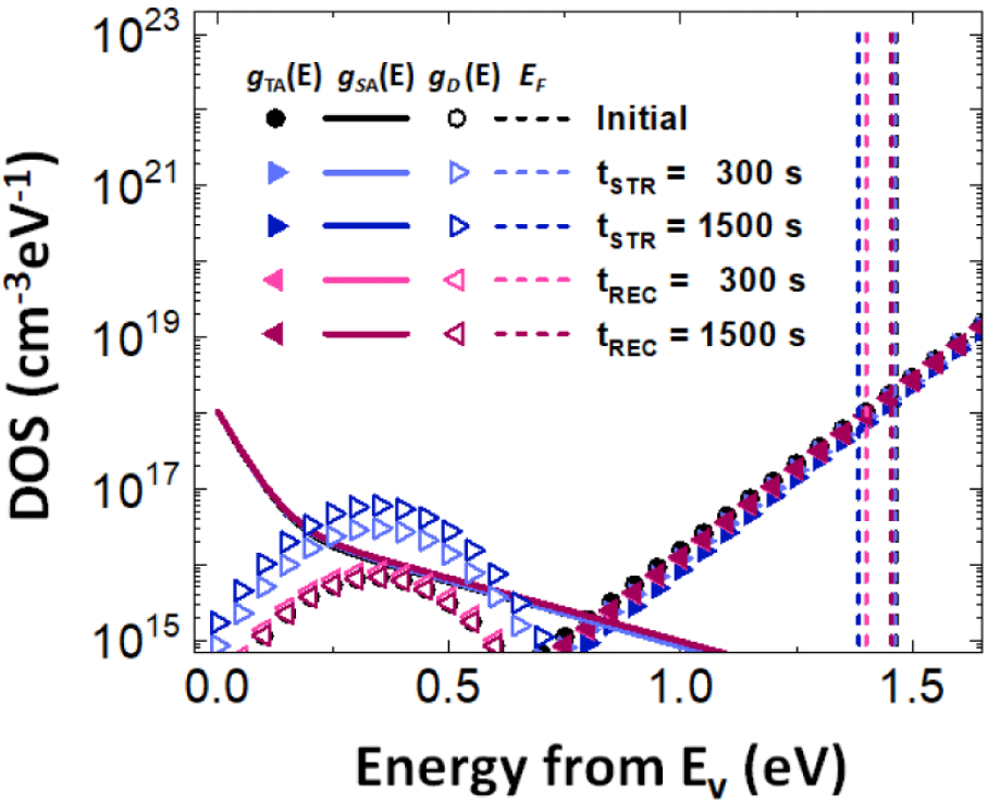
Fig. 4(a) shows the portions of the total VT occupied by each parameter extracted from the I–V modeling and the DOS profile to visualize the effect of each parameter on VT. The quantity ΔVOX corresponds to the interaction between the charge carriers and the subgap states within the gate insulator. The quantities ΔVGSA(E) and ΔVgD(E) are associated with the interactions with the electron-acceptor states and the hole-donor states, respectively, within the active layer. As shown in Fig. 4(a), ΔVOX and ΔVGSA(E) mainly affect the shifts of VT during the PBS and the recovery time. However, the effect of ΔVgD(E), which corresponds to the interaction with hole-donor states, is negligible. Fig. 4(b) shows the changes in ΔVT as a function of time in the inkjet-printed PTFT, which was first stressed with VG= −20 V and VD=−1 V for 1,500 s, after which the stress was removed. We monitored the changes in ΔVT by collecting transfer characteristics over the range from VG=20 V to –20 V, with VD=–10 V, at time intervals determined more frequently than in Fig. 2(c). As the duration of the PBS increases, the VT of the PTFT shifts in the positive direction. At the beginning of the recovery process, VT first shifts rapidly in the negative direction, but the shift gradually slows down and eventually remains at an irreversible point with increasing recovery time. We fitted ΔVT for the PBS and recovery process to the respective functions ΔVT(t)=ΔV0 {1 – exp [–(t/τ)β]} and ΔVT(t)=ΔVmax exp [−(t/τ)β] [17,18]. Here, ΔV0=VG–VT0, where VT0 is the initial threshold voltage, ΔVmax is the value of ΔVT right before the recovery begins, β is the dispersion parameter, and τ is the charge trapping/ detrapping time constant. The fitted values of β and τ are 0.88 and 631 s for PBS and 0.17 and 2,990 s for the recovery process, respectively.
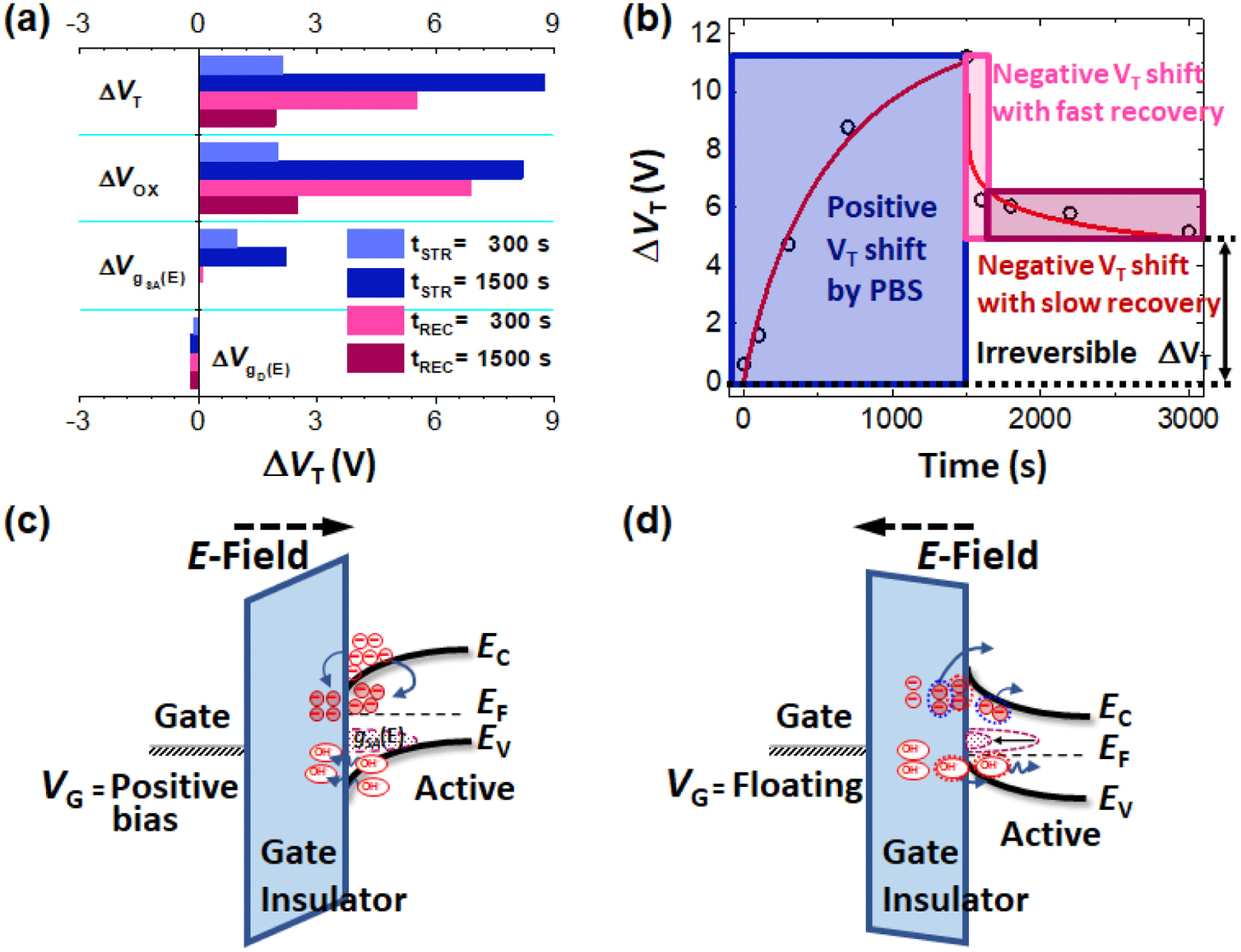
Based on these observations, the physical mechanisms for the changes in the PTFT ΔVT during the PBS and the recovery process can be expressed schematically as shown in Fig. 4(c) and Fig. 4(d), respectively. First, the positive direction shifts of ΔVT observed in the PTFT under PBS conditions can be explained by four processes: (i) Electrons are induced at the interface between the insulator and the channel by the positive bias applied to the gate, and most of the induced electrons are injected into the insulator by the electric field and are drawn toward the active layer. (ii) Some of the induced electrons at the interface diffuse to and are trapped in the shallow states near the EC. (iii) Some anions (OH−), which decompose from the moisture (H2O) in the air, are absorbed by the polymer layer and are attracted by the positive VG, resulting in the generation of defect states [gSA(E)] near EV. (iv) Some OH− ions migrate to the insulator under the influence of the electric field. Conversely, the recovery of ΔVT caused by releasing the VG applied to the PTFT is divided into a fast recovery step and a slow recovery step, each of which can be described as two sequential processes: (v) Electrons trapped in the shallow trapping states near EC are immediately detrapped by the electric field applied to the insulator by the floating gate. (vi) When the PBS is removed, most of the OH− ions that had been attracted to the gSA(E) within the active layer are pushed away from the interface and migrate to the back channel. During this process, the gSA(E) generated by the OH− ions are annihilated as those ions move away. (vii) Most of the OH− ions trapped inside the insulator by PBS gradually out-diffuse toward the channel through the insulator/active interface. (viii) Some trapped OH− ions in the insulator remain even after the PBS is removed, leading to the irreversible component of ΔVT. In addition, some OH− ions that migrated to the polymer film also can react with the conjugated polymer chain and induce bipolaron states [19].
4. CONCLUSION
We have investigated the effects of bias stress in an inkjet-printed P8T2Z-C12 PTFT in terms of the subgap DOS. Under PBS conditions, the VT of the PTFT shifts in the positive direction while generating defect states in the subgap DOS of the active semiconducting polymer layers. However, this shift in VT is mostly recovered when the PBS is removed. We also confirmed experimentally that the defect states in the subgap DOS annihilated during the recovery process.