1. INTRODUCTION
The rapid advancements in artificial intelligence technology have ushered in the era of Big Data, resulting in an increased demand for faster and more energy-efficient data processing technologies [1]. However, the traditional CMOS-based Von Neumann architecture, wherein the processing unit and memory devices are connected via a data bus, faces a bottleneck issue due to its sequential computation process [2]. Recently, there has been much attention directed towards neuromorphic computing systems, which aim to emulate the functionality of the human brain in order to achieve energy-efficient and rapid processing [3]. The human brain, consisting of approximately 1011 neurons interconnected via around 1015 synapses, processes and stores information by modulating synaptic weights through bioelectrical signals. In such biological systems, parallel computation is achieved by signals transmitted along synapses, with each signal consuming only about ∼1 fJ, thereby exhibiting rapid operation with high energy efficiency [4]. To realize practical neuromorphic systems, it is imperative to develop artificial synapses with functions similar to their biological counterparts [5]. In nervous systems, synaptic weights between neurons are continuously tuned by history-dependent external stimuli, following Hebbian learning rules including synaptic plasticity. To date, numerous approaches have been explored for developing synaptic devices to emulate Hebbian learning rules in hardware computing systems [6-9].
A 3-terminal synaptic transistor stands out as a promising candidate for artificial synapses due to its ability to achieve precisely tunable memory states [10,11]. In synaptic transistors, the application of external electric signals to a gate electrode induces a change in the channel conductance. Various operating principles, such as phase change, charge or ion-trapping, and ferroelectric phenomena, have been investigated for the development of synaptic transistors [12-15]. Among these synaptic transistors, ferroelectric synaptic transistors, which utilize a ferroelectric dielectric layer as a gate insulator, offer fast switching speeds, low energy consumption, and multilevel memory states through spontaneous polarization switching, making them promising components for artificial synapses [16]. In the realm of ferroelectric field effect transistors, a variety of ferroelectric dielectric layers, ranging from oxide films to organic materials, have been utilized [17-20]. In oxide materials, film deposition processes have typically demanded high temperatures (exceeding 230°C), making them unsuitable for flexible substrates such as polyimide and poly (ethylene naphthalate)[21]. In contrast, ferroelectric transistors based on organic materials can be fabricated using straightforward low-temperature solution processes (below 230°C), rendering them ideal for flexible electronics [19,22-26].
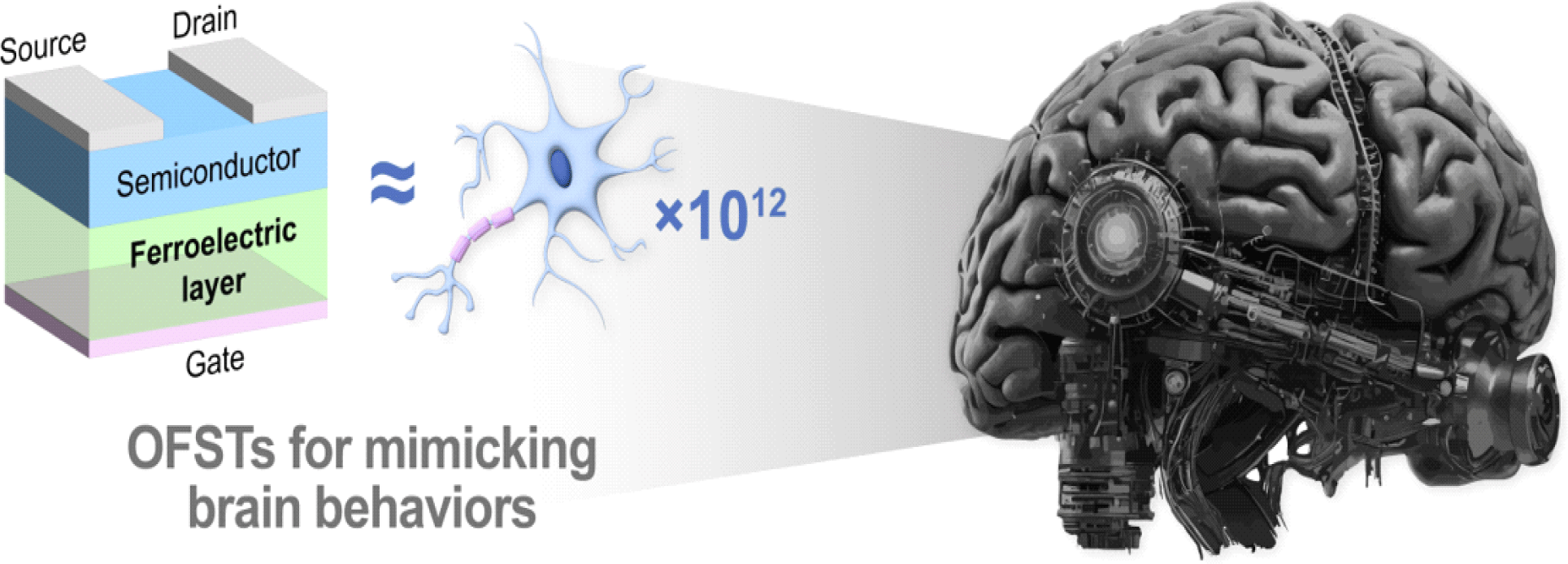
Organic ferroelectric synaptic transistors (OFSTs) provide promising capabilities for advancing practical applications in wearable electronics, such as flexible parallel computation and artificial sensory nervous systems, due to their reliable performances [23-26]. Several studies have been conducted in the replication of synaptic functions in OFSTs by manipulating the dipole switching dynamics within a ferroelectric polymer layer (Fig. 1) [23-28]. Nevertheless, achieving OFSTs with bio-realistic synaptic functions remains difficult. Moreover, the development of wearable neuromorphic systems capable of computing at levels akin to the human brain poses significant challenges. To realize smart wearable systems capable of efficiently processing vast amounts of data, it is imperative to develop artificial synapses that emulate complete synaptic functions [29,30]. These functions should encompass synaptic plasticity, multilevel memory states, low operating voltage, and multifunctional capabilities. While the development of flexible OFSTs with comprehensive synaptic functions is crucial, there has been a lack of specific discussion on the direction and perspectives for studies in this area.
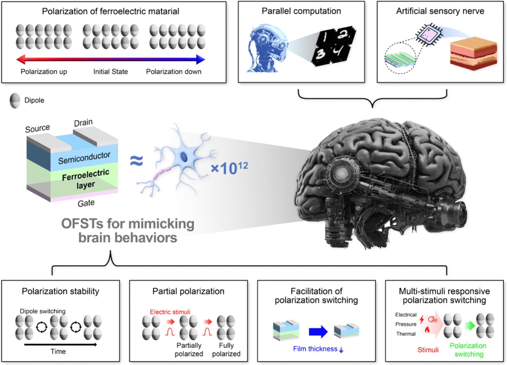
In this paper, we explore recent approaches to manipulate the dipole switching dynamics in OFSTs for emulating synaptic functions. Additionally, we propose future directions for developing wearable neuromorphic systems. Initially, we elucidate the physical background to understand the dipole switching dynamics relevant to the memory effects of OFSTs. Secondly, we examine the methods for replicating biological functions, including synaptic plasticity, analog memory states, low operating voltages, and multifunctional capabilities for sensing and memory, in the flexible OFSTs. Subsequently, we explain applications for the flexible neuromorphic systems based on OFSTs, such as parallel computation and sensory nervous systems. Finally, we propose insights into the application of flexible OFSTs for wearable smart systems.
2. DIPOLE SWITCHING IN OFSTs
Ferroelectric synaptic transistors utilize a ferroelectric layer as a gate insulator, where the dipoles within the ferroelectric insulator are permanently aligned by a gate bias, as shown in Fig. 2(a). This alignment leads to either an increase or decrease in the channel conductance of the device [31]. In a writing or erasing process, applying a gate bias exceeding a specific voltage known as the coercive voltage induces spontaneous polarization switching of the dipoles within the ferroelectric layer, either upward or downward. The polarization switching results in charges being bound at the interface between the ferroelectric and semiconducting layers. This phenomenon leads to the accumulation or depletion of mobile charges in the semiconductor, consequently increasing or decreasing the channel conductance of the device. For instance, in the case of n-type ferroelectric transistors, positive and negative gate voltages respectively enhance and degrade the channel conductance (Fig. 2(b) [16,31]. In a reading operation, we can check the memory state (channel conductance state) of the device by applying a small drain voltage, about 5 V, at 0 V of both the source and gate biases. The electrically controllable characteristics of channel conductance in ferroelectric synaptic transistors are analogous to synaptic weights tuned through external stimuli in biological systems [32].
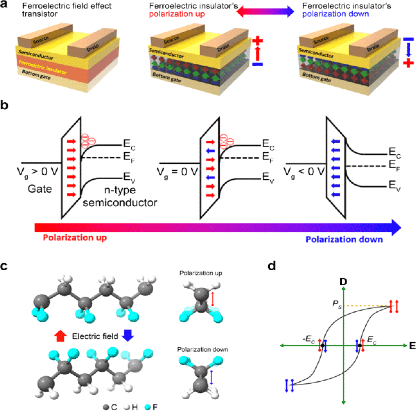
Polyvinylidene fluoride (PVDF) and PVDF copolymers have been utilized as ferroelectric layers in the OFSTs, owing to their thermal stability, biocompatibility, and mechanical flexibility [33,34]. PVDF, composed of repeating molecular units of (CH2-CF2), can crystallize into various phases, including α-, β-, γ-, and δ-phases. In the β-phase, PVDF and PVDF copolymers demonstrate reversible and permanent polarization switching characteristics under an external electric field, resulting in ferroelectric behavior (Fig. 2(c)). Typically, PVDF films produced by solution processes result in the α-phase, which lacks polar characteristics. Additional mechanical deformations or high-temperature thermal processes are necessary to induce the formation of the β-phase, which exhibits ferroelectric properties [35].
Poly (vinylidene fluoride-trifluoroethylene) (P(VDF) -TrFE) copolymer has recently gained widespread use as an organic ferroelectric layer due to its ability to readily crystallize into a ferroelectric phase resembling that of β-PVDF [36,37]. In P (VDF-TrFE), with units comprising (CH2–CF2) and (CF2–CHF), the CH2 and CF2 groups rotate along the carbon backbone under an electric field, resulting in the alignment of dipoles. The electric field required to induce the polarization switching is referred to as the coercive field. Furthermore, the ferroelectric polarization saturates at a specific value with increasing electric field, and this polarization is retained remanently when the electric field is removed, as presented in Fig. 2(d) [34,38].
3. CONTROL Of Dipole Switching Dynamics In Ofsts For Artificial Synapses
To achieve energy-efficient learning processes in hardware neuromorphic systems, synaptic plasticity from biological synapses should be fully emulated in the artificial synapses [3]. In biological systems, synaptic plasticity can be classified into two distinct functions: the first entails short-term plasticity (STP), which persists for several seconds to minutes, while the second involves long-term plasticity (LTP), enduring for several hours or more [8]. STP and LTP manifest independently and are correlated with each other for performing timing-dependent learning processes [39-41]. STP temporally adjusts synaptic weights in response to input stimuli, while LTP induces permanent modifications based on the timing of sequential stimuli. In the OFSTs, memory retention properties are primarily governed by a depolarization field (Edep), which relaxes the switched dipoles back to their initial state [16,27]. In ferroelectric dielectric layers, Edep typically arises from non-ideal screening of bound polarization charges at the electrodes, inducing polarization inversion in OFSTs due to its counter polarity with the electric field responsible for spontaneous polarization switching. Thus, the Edp can be used as a critical factor for emulating synaptic plasticity in the OFSTs.
As the charge screening to suppress the Edep is intensified by the electric field in a ferroelectric layer, several studies have been performed to modulate the conditions of electric signals applied at a gate electrode to selectively achieve STP and LTP in the OFSTs [22-25]. In the P(VDF-TrFE)-based OFSTs employing a pentacene semiconducting layer, STP and LTP were sequentially implemented through the duration of a single gate pulse and the time interval between repeated gate pulses [22]. As the duration of the gate pulse increased, charge screening was achieved more effectively, weakening the Edep for dipole relaxation and resulting in a shift in memory retention characteristics from STP to LTP (Fig. 3(a)). Additionally, a shorter interval between the repeated pulses leads to complete polarization switching with high stability, similar to LTP (Fig. 3(b)). Moreover, as shown in Fig. 3(c), the increased channel conductance was saturated upon full polarization switching, effectively emulating homeostatic feedback that inhibit the overgrowth of synaptic connections in biological systems [42]. However, this device exhibited incomplete synaptic plasticity, comprising dependent STP and LTP. Consequently, additional pulse engineering schemes were necessary for pulse-based learning processes, such as spike rate-dependent plasticity and spike timing-dependent plasticity.
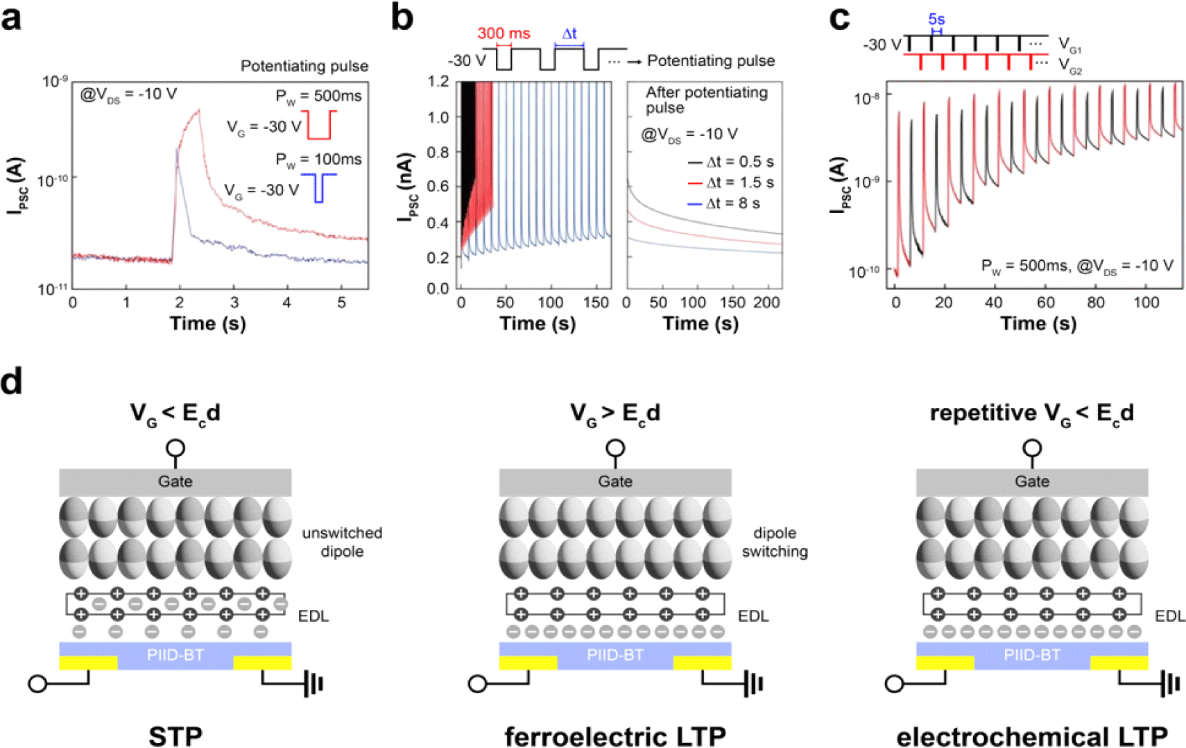
To represent the independent STP and LTP characteristics in the OFSTs, multi-stacked gate dielectric layers consisting of P (VDF-TrFE) and poly[(1-vinylpyrrolidone)-co-(2-ethyldimethylammonioethyl methacrylate ethyl sulfate)] (P(VP-EDMAEMAES)) were utilized [25]. In this device structure, the electrochemical and ferroelectric switching behaviors, analogous to STP and LTP respectively, were independently achieved at different gate voltage amplitudes, as shown in Fig. 3(d). When a gate bias of the OFST with the multi-stacked gate insulators was lower than the coercive voltage for the P (VDF-TrFE) film, mobile ions from P (VP-EDMAEMAES) migrated to a semiconducting layer of poly (isoindigo-co-bithiophene), doping the channel region and inducing STP characteristics with a temporary increase in channel conductance. Conversely, a gate voltage exceeding the coercive voltage triggered polarization switching for LTP lasting several hundred seconds, in the device. Although this device exhibited the independent STP and LTP properties stemming from the different operating principles, not only polarization switching but also ion-doping processes were enhanced at higher gate voltages, potentially compromising the reliability of synaptic plasticity.
In the human brain, computational processes occur in parallel through the interactions of signals flowing along neurons connected via synapses [43-48]. During this process, continuous values for synaptic weights facilitate rapid and complex computations. For hardware neural networks, achieving multilevel memory states, akin to analog states, in artificial synapses is crucial for computational accuracy and integration density [4,49]. In OFSTs, the channel conductance serves as a synaptic weight, which can be tuned by the polarization state of the ferroelectric gate insulator [28]. Various approaches have been performed for achieving multilevel conductance states in OFSTs by controlling dipole switching [28,50].
Repeated gate voltage pulses have been extensively utilized to achieve multilevel conductance states in the OFSTs [28]. The number of pulses was controlled to modulate dipole switching, thereby regulating the resultant channel conductance in the devices. However, in this approach, the polarization switching occurs abruptly, leading to nonlinear conductance changes that limit the number of achievable conductance states in the devices. To achieve gradual dipole switching, non-identical gate pulses were sequentially applied to the OFST comprising a P (VDF-TrFE) gate insulator and a graphene oxide semiconductor [50]. In this research, the polarization switching was finely controlled by gradually increasing pulses from 0.255 V to 0.500 V, as confirmed by the linear increase in channel conductance of the synaptic device.
Rather than employing complex pulse tailoring, the device configuration can be engineered to enhance the effect of polarization switching on channel conductance changes, thereby enabling gradual control of the conductance through the identical voltage pulses [51,52]. A vertically structured OFST was developed, comprising a silicone gate electrode, silicone dioxide gate insulator, P (VDF-TrFE) ferroelectric gate insulator, Ag nanowires source network electrode, and Ag drain electrode, to achieve polarization switching, which significantly impacts channel conductance [51]. In this vertical configuration, the channel length was designed at the nanoscale (approximately 120 nm), resulting in the low sub-threshold swing and the high channel conductance variation, defined as the ratio of maximum to minimum conductance in the device. Compared to a conventional lateral-structured device with the poor conductance variation (about 6.7), the vertical OFST exhibited a more gradual change in conductance at the repeated identical pulses due to the enhanced dipole switching effect resulting from the higher conductance variation (about 16.9). Recently, a Pd source electrode with a high barrier height for carrier injection was introduced in the P (VDF-TrFE)-based OFSTs with a semiconducting layer of molybdenum disulfide (MoS2), aiming to reduce the off-current value and achieve the high channel conductance variation [53]. In this synaptic device, a relatively linear change in the weight was confirmed under the constant gate pulses compared to the reference devices with lower carrier injection barriers, as presented in. Despite these considerable efforts to develop OFSTs with continuous multilevel conductance states, emulating the biological synaptic weight remains challenging. Specifically, in the OFSTs, intermediate conductance states attributed to the partial polarization switching exhibit poor stability, closer to STP than LTP [54], making it difficult to utilize these states in parallel computation. However, previous studies have not clearly demonstrated stable retention performances for multilevel conductance states.
To use a flexible OFST as a practical component in wearable electronics, it is essential to explore strategies aimed at reducing the device’s operating voltage to levels comparable to biological systems [34,55-58]. In ferroelectric transistors, such as OFSTs, the coercive voltages can be decreased by employing thinner ferroelectric films [59-61]. However, in the case of organic ferroelectric layers, reducing the thickness can degrade crystallinity, consequently augmenting the Edep and compromising the polarization stability necessary for LTP. Furthermore, developing OFSTs with a ferroelectric film thinner than one hundred nanometers is barely possible due to the high leakage current issues.
To mitigate the polarization switching voltages in OFSTs with a gate insulator thick enough to circumvent leakage current issues, a method involving blending a high-k material into the ferroelectric polymer layer was proposed [62]. In OFSTs incorporating a blend of P (VDF-TrFE) with a high-k polymer, poly (vinylidene-fluoride–trifluoroethylene–chlorotrifluoroethylene) (P (VDF-TrFE-CTFE)), polarization switching was achieved at a relatively low voltage (about 12.1 V), in contrast to typical devices comprising solely the P (VDF-TrFE) film (about 15.7 V). This improvement can be attributed to the enhanced film capacitance, which facilitates dipole switching.
To bring down the operating voltages of OFSTs to levels comparable with commercial standards, multi-stacked ultrathin films have been employed as gate insulators [17,26,60,63]. Utilizing an ultrathin ferroelectric polymer with high-k properties, P (VDF-TrFE-CTFE), as the gate insulator, along with additional AlOx interfacial layers sandwiching the gate insulator, was introduced to reduce the polarization switching voltage and mitigate gate leakage current (Fig. 4(a))[63]. As shown in Fig. 4(b), this OFST demonstrated reliable polarization switching at a low voltage of 4 V, along with stable retention performance for channel conductance states. The high dielectric constant (k=∼28) of the ferroelectric film facilitated polarization switching and mitigated the Edep. Furthermore, the interfacial AlOx films effectively acted as blocking layers to suppress leakage current, as presented in Fig. 4(c).
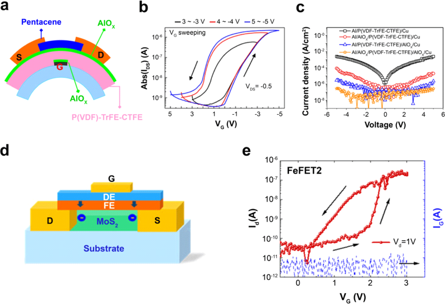
Recently, an approach has been explored to enhance the impact of polarization switching on channel conductance while simultaneously facilitating dipole switching, aiming to regulate the conductance of OFSTs at low operating voltages [26]. As the gate insulating and semiconducting layers, a multi-stacked thin film consisting of a P (VDF-TrFE) ferroelectric layer and an Al2O3 insulating layer, and MoS2 2D semiconductor with high carrier mobility, were employed, respectively (Fig. 4(d)). In this OFST, the combination of the effects from the low thickness (10 nm) of the ferroelectric layer and the superior sub-threshold swing of the MoS2 channel resulted in a reduction of the polarization switching voltage to approximately 3 V (Fig. 4(e)). In addition, stable conductance retention performance was implemented by optimizing the Al2O3 film thickness to minimize the Edep.
To design highly integrated neuromorphic systems, multifunctional synaptic devices that can act as both sensor and memory components have been studied [64-67]. For the OFSTs, several types of multifunctional synaptic devices have been developed to effectively process mechanical and optical signals [19,24,68-70]
For the P (VDF-TrFE)-based tactile OFST, a dome-shaped gate electrode with mechanically deformable characteristics was fabricated using a polydimethylsiloxane film coated with the conducting polymer poly (3,4-ethylenedioxythiophene)-poly (styrenesulfonate) (Fig. 5(a))[69]. As the magnitude of the pressure stimulus increased, the contact area of the gate electrode on the ferroelectric layer expanded due to electrode deformation, leading to polarization switching in more domain regions under a constant gate bias (Fig. 5(b)). This synaptic device demonstrated tactile-stimuli responsive dipole switching and the resultant conductance modulation, as shown in Fig. 5(c).
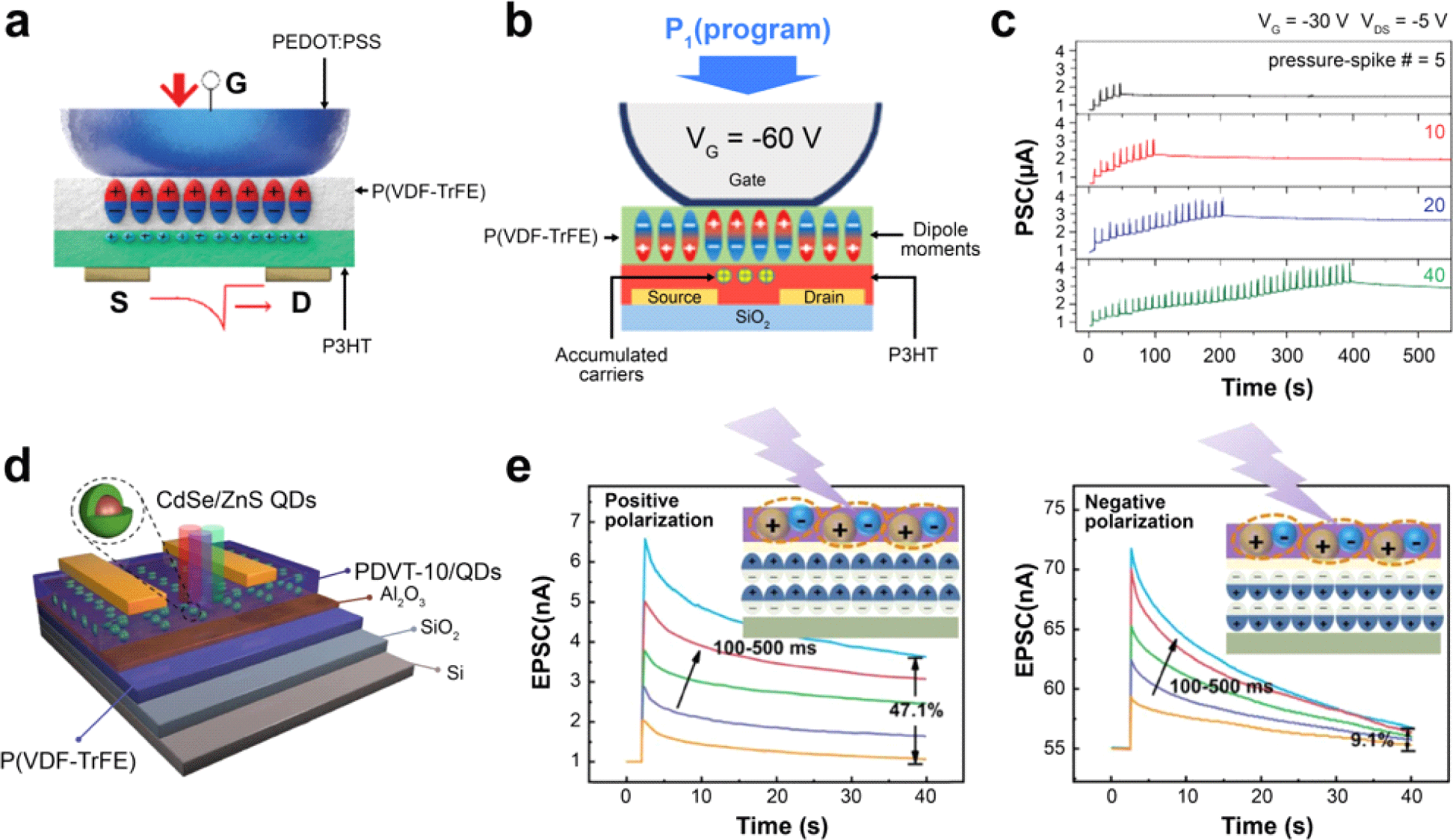
The incorporation of additional doping of quantum dots (QDs) into a semiconducting layer can provide the construction of photo-responsive OFSTs, as presented in Fig. 5(d)[70]. In the OFST consisting of a P (VDF-TrFE) ferroelectric layer and a CdSe/ZnS QD-doped semiconductor, poly[2,5-bis(alkyl)pyrrolo[3, 4-c]pyrrole-1,4(2H,5H)-dione-alt-5,5’-di(thiophen-2-yl)-2,2’-(E)-2-(2-(thiophen-2-yl)vinyl)thiophene], the photo-responsive synaptic characteristics were emulated by the interactions between polarization switching and the photo-generation of electron-hole pairs (Fig. 5(e)). When the gate bias exceeded the coercive positive voltage, the device underwent positive polarization. In this state, the device exhibited a permanent change in channel conductance, with an increase in trapped electrons in the channel in response to ultraviolet light stimuli. In contrast, the device in the negative polarization state exhibited volatile photogenerated currents, attributed to the photo-generated electron-hole pairs from the QDs and their potential recombination.
4. WEARABLE NEUROMORPHIC SYSTEMS BASED ON OFSTs
Parallel computation is a versatile approach used to evaluate the potentials of synaptic devices and arrays. For such rapid computing processes, non-volatile multilevel memory states in artificial synapses are essential for training the device according to offline learning rules [71]. The OFSTs can be played as a synaptic component in the wearable computation systems, in terms of their mechanical flexibility, and multilevel conductance states. A study has been conducted to construct parallel computation systems compatible with flexible substrates, using the OFSTs with the P (VDF-TrFE) ferroelectric films and MoS2 semiconducting layers [26]. In this study, based on the synaptic characteristics of OFSTs, numerical simulations were performed to construct computing systems for recognizing handwritten digit images from the Modified National Institute of Standards and Technology database, as presented in Fig. 6(a). The constructed systems demonstrated high accuracy in recognizing the images, comparable to that of ideal software (Fig. 6(b)). However, variations in repeated switching operations and device-to-device uniformity were not precisely reflected in this analysis.
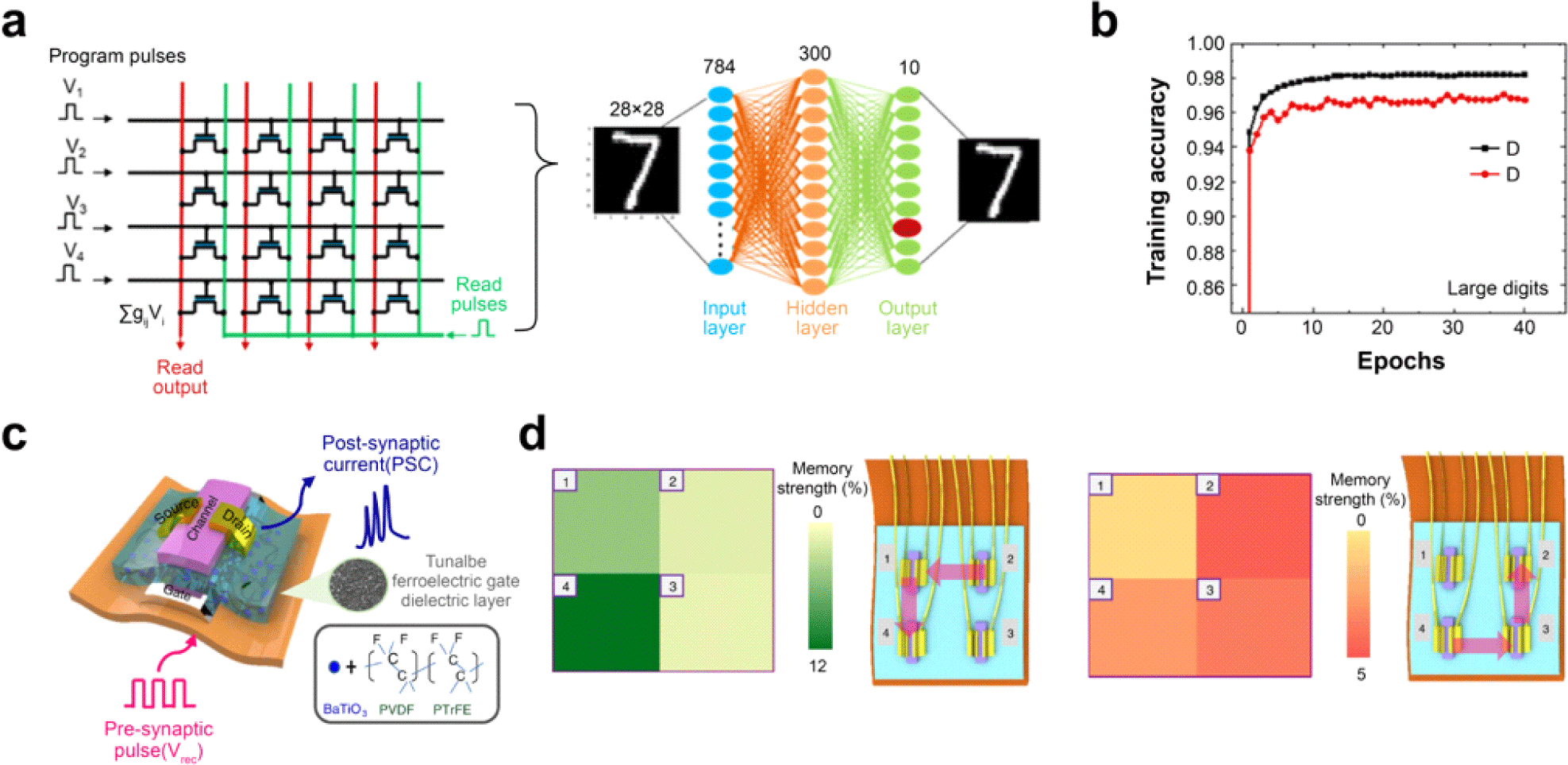
The artificial sensory nervous systems are critical applications of synaptic devices for presenting the capabilities for smart robotics and prosthetics [72]. Various studies have been conducted to demonstrate artificial sensory nervous systems, including synaptic tactile sensory organs and artificial visual-perception systems, utilizing the OFSTs with mechanical flexibility and synaptic functions [24,25]. The tactile OFST with a barium titanate nanoparticle-doped P (VDF-TrFE) layer was prepared on a flexible polyimide substrate, as shown in Fig. 6(c)[24]. A triboelectric effect was induced at the Ni gate electrode through mechanical stimuli on the substrate, effectively emulating the behaviors of tactile sensory organs (Fig. 6(d)). Additionally, an organic photodetector can be serially integrated with OFSTs to achieve a flexible visual-perception system [25]. The flexible visual-perception system, involving dioctyl-substituted perylene tetracarboxylic diimide-based photodetectors and P (VDF-TrFE)-based OFST arrays, exhibited selective photo-responsive synaptic characteristics according to optical wavelength. In these approaches, each system was operated stably as the artificial sensory nerve with mechanical flexibility. However, the intrinsically flexible characteristics, similar to biological nerves, were not completely achieved due to the rigid properties of the electrodes.
5. PERSPECTIVE AND FUTURE PROSPECTS
Here, studies on OFTSs for achieving flexible synaptic components in wearable neuromorphic electronics have been reviewed, ranging from the device level to system level. Basic information for understanding the operating mechanisms of the devices and the organic materials used for preparing ferroelectric dielectric layers is explained. Polarization switching is a crucial factor that determines the change in channel conductance in response to electric stimuli, in OFSTs. To mimic synaptic behaviors such as synaptic plasticity, continuous synaptic weight, low operating voltage, and multifunctional characteristics, many studies have been conducted to precisely control the dipole switching dynamics in OFSTs. However, bio-realistic synaptic functions have not yet been achieved in these devices, restricting the realization of practical neuromorphic systems compatible with wearable electronics. Specifically, the complete synaptic plasticity, consisting of independent STP and LTP properties, is required be emulated in OFSTs to follow history-based learning rules with high energy efficiency. In addition, the retention performance of the conductance states should be considered when engineering dipole switching in the devices to achieve multilevel conductance states and low voltage operation. Partial dipole switching related to intermediate states, which can contribute to multilevel conductance states and low voltage operation in the OFSTs, possesses a relatively unstable polarization state. This instability can lead to poor retention performance in the devices. Moreover, further studies to improve the fluctuations during repeated device operations and to enhance device-to-device uniformity should be conducted in OFSTs, in order to develop practical applications involving highly integrated synaptic arrays, beyond simulation analysis. Lastly, it is important to develop strategies for fabricating OFSTs with intrinsic flexibility, approaching the level of biological counterparts, to realize wearable or stretchable artificial nervous systems.


